CXL_Cluster V3P1 IP
Features:
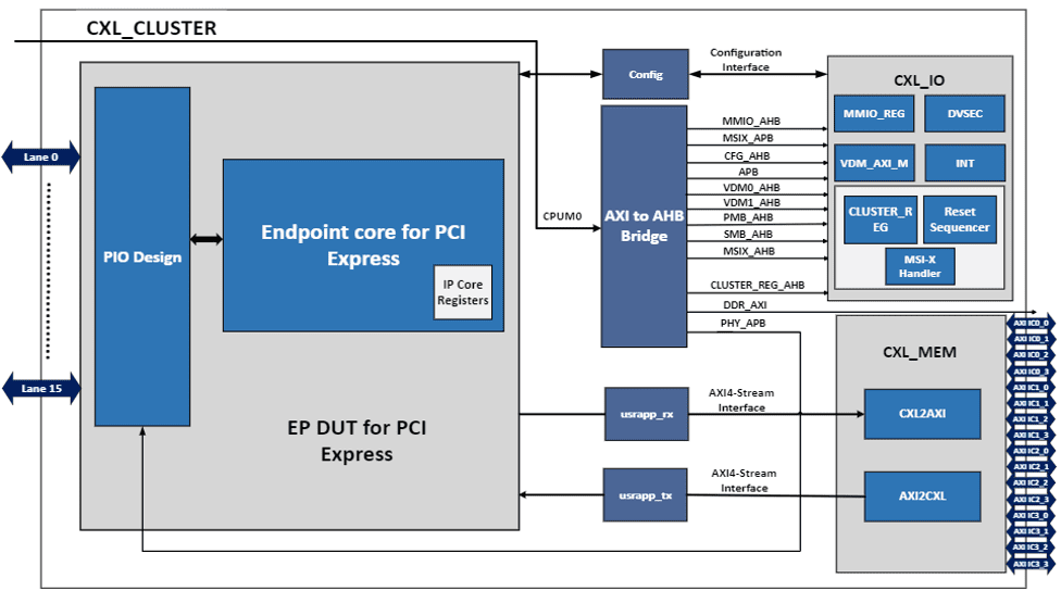
- Based on PCIe Gen5 64GT/s, Total 16 lanes
- PCIe 4 links of x4 lanes can be configured as 1 x16
- Vendor-Specific Extended Capability (VSEC) registers are provided
- Designated Vendor-Specific Extended Capability (DVSEC) registers are provided
- AXI-Lite and AHB interface for Configuration space register access
- AXI-Lite interface to access DVSEC registers
- Message Signal Interrupt Extended (MSI-X) support
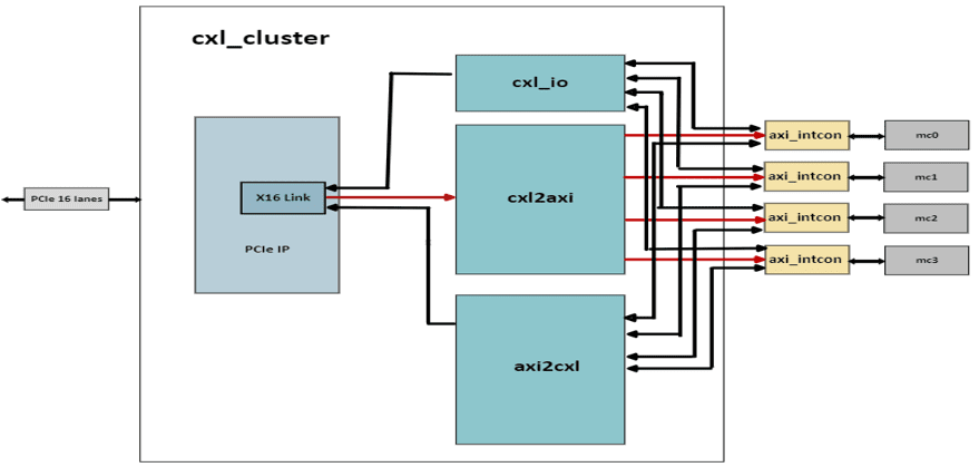
- AXI fabric operates at 256 bits, with rate adaptation to 256 bits and four separate ports
CXL.io V3P1 IP
Features:
-
CXL 3.0 Compliant with IDE
-
Based on PCIe Gen6 64GT/s, Total 16 lanes
-
PCIe 4 links of x4 lanes can be configured as 1 x16 or 2 x8
-
Bandwidth adjustment based on system needs
-
Vendor-Specific Extended Capability (VSEC) registers are provided
-
4 Links of x4 can be integrated to generate x16 lane interface
-
Designated Vendor-Specific Extended Capability (DVSEC) registers are provided
-
AXI-Lite and APB interface for Configuration space register access
-
AXI-Lite Snoop interface to access DVSEC and CLDAT registers
-
Message Signal Interrupt Extended (MSI-X) support
CXL.mem V3P1 IP
Features:
- Max Throughput: 64 GB/s
- Memory Size per AXI Port (DDR Subchannel): Up to 256 GB
- Number of CXL Ports: 1
- Number of LDIDs per CXL Port: Up to 4
- Number of HDM Decoders per LDID: Up to 4
- Number of m2s Requests per Tick: Up to 2 m2s_rwd and 2 m2s_req
- Interleave Ways of HDM Decoder: 2, 4, 8, 16
- Interleave Ways of AXI Ports (DDR Subchannels): 3, 6, 12
- Interleave Granularity of HDM Decoder: 256 B, 512 B, 1 KB, 2 KB, 4 KB, 8 KB, and 16 KB
- Interleave Granularity across AXI Ports (DDR Subchannels): 64 B, 256 B, and 1024 B
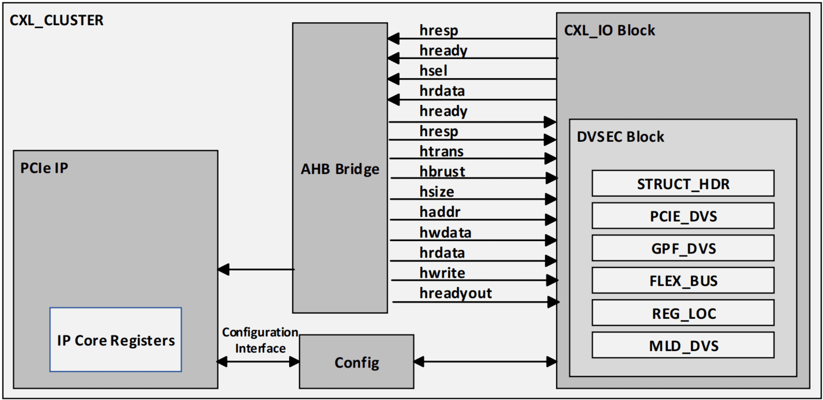
CXL.io MMIO Register Set IP
Features:
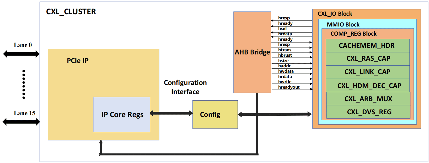
- CXL.io supports PCIe/CXL X16 Link.
- CXL.io block provides AHB interfaces to access MMIO space registers.
- Registers can be access indirectly through the PCIe link from the host.
- Vendor-Specific Extended Capability (VSEC) and Designated Vendor-Specific Extended Capability (DVSEC) registers are provided
- AXI4 and AHB interface for Configuration space register access
CXL Component Register Set IP
Highlights:
- Simplifies device configuration and management.
- Enhances interoperability between devices and host systems.
- Enables efficient communication and resource utilization.
- Promotes CXL technology adoption and innovation.
CXL Designated Vendor Specific Extended Capability Register Set IP
Features:
- Customized Capabilities: For flexibility, accommodating a variety of use cases and specialized hardware.
- Extended Capabilities: Including specialized control registers, feature flags, or configuration settings specific to the device or vendor.
- Device Identification and Configuration: To recognize the device, access its specific features and configure its behavior.
- Vendor-Specific Features: Including enhanced security measures, unique data processing capabilities or specialized data transfer modes.
- Interoperability Support: It ensures not to disrupt the fundamental compatibility and interoperability of device across different vendors
- Programming Interface: To interact with the vendor-specific functionalities of a devices.
- Compliance and Standards: To ensure compatibility and compliance with the broader CXL ecosystem.
- Future-Proofing and Extensibility: For future enhancement and extension without requiring a complete overhaul of the CXL standard.
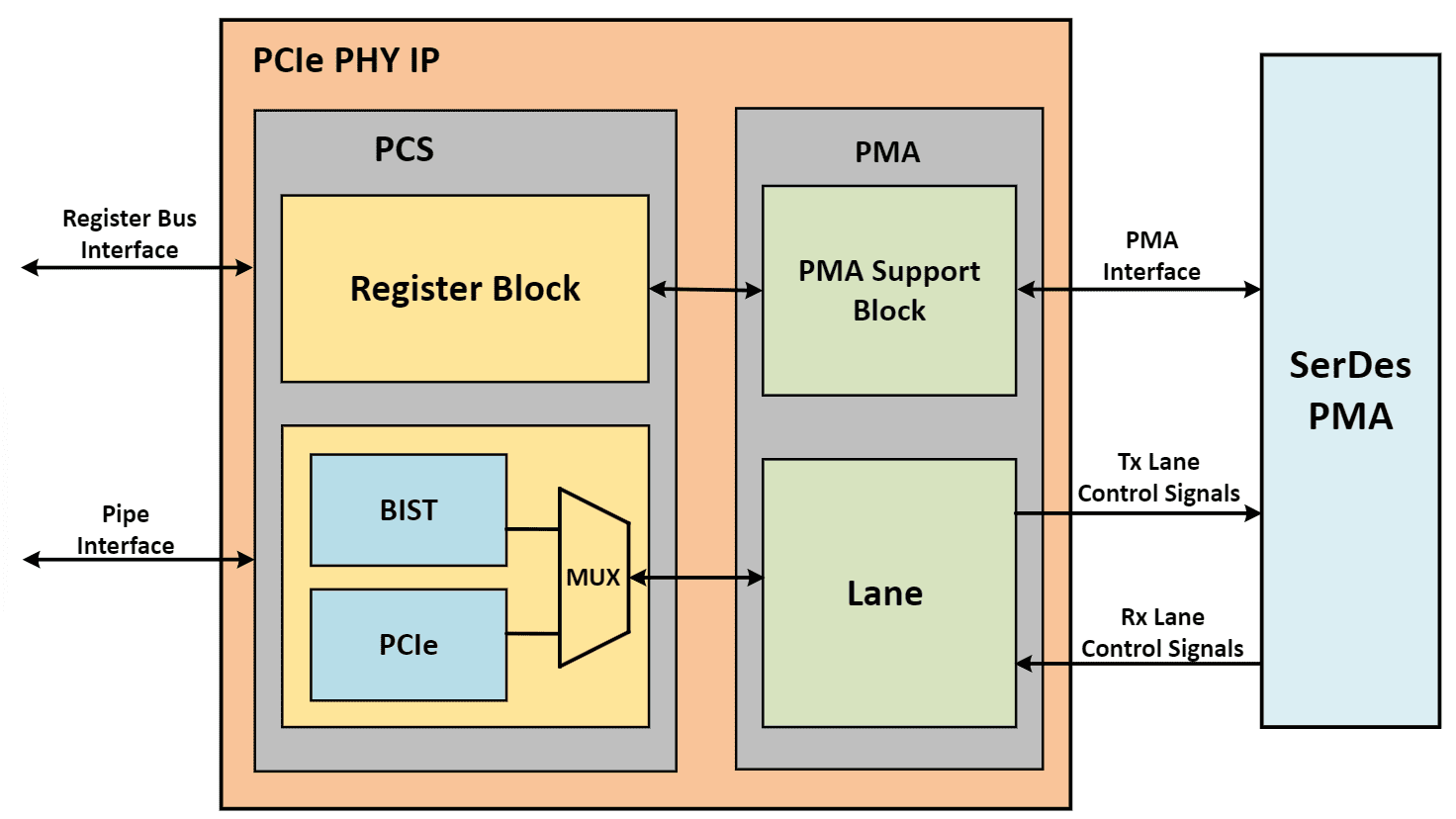
PCIe Gen4 PHY IP
Features:
- Physical Coding Sublayer (PCS) block with PIPE interface
- Lane Margining at the receiver
- Fixed PMA data symbol width
- PIPE bifurcation for up to 16 lane PHY configurations
- Continuous time linear equalizer with programmable settings.
- Spread-spectrum clocking
- Transmitter performance under low-supply conditions.
- Data and clock recovery under low-supply conditions.
External Memory Interface IP
Features:
- Boundary scan
- Access from CPU1 to CPU6 Fast access to 3 Primary CPUs (1,3) 1 pipeline in forward path to CPUs (2)
- Access from RTDMA 1 pipeline in for forward path Burst support with Look ahead address generation
- For Large transfers / Copy use of RTDMA is recommended
- Separate Buffer Module (with data line buffer and Write FIFO) for each CPU All reads to External Memory Interface forced to be 64-bit accesses. Data line buffer can be bypassed using alternate memory map Write FIFO can contain up to 4 entries
- 64-bit access from initiator will be cause a Peripheral Bus-burst 2×32 bit accesses on the Peripheral Bus External Memory Interface IP further splits accesses based on External Memory Interface IP data size (16/32 based on Narrow Mode config for SDRAM, 8/16/32 based on Size config for ASRAM).
-
Accesses from different initiators are arbitrated in round-robin
-
Accesses from same initiator arbitrated in Fixed priority
-
Supports single chip-select (CS0) for SDRAM, four chip-selects (CS1-CS4) for ASRAM, and an additional range for External Memory Interface IP register accesses
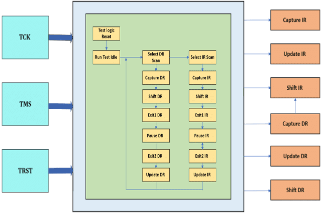
JTAG Tap Controller IP
Features:
- Boundary scan
- Device and design verification
- Switching to special CPU or chip modes
- Configuring the JTAG chain
- Communication with special devices accessible via a JTAG TAP
- Remote API
- JTAG commands
- Support for High-Performance Systems

